Zedboard Hardware Peripheral Mapping
In this document you will find the default hardware mapping on the Zedboard when using the provided pre-loaded SD Card.
The hardware peripherals are implemented in the FPGA, also called PL (programmable logic) side in the Xilinx reference document terminology. Each peripheral has a base address that can be found in this document. These pebashripherals are mapped to board resources e.g. LEDs, switches, headers which will be used to perform the experiments in the assignments.
Hardware peripheral table
All peripherals are configurable, and memory mapped to a certain memory region. You will need to get more information on the respective hardware cores in order to employ them. Please refer to the reading list.
| Base Address | Peripheral Type | Description |
|---|---|---|
| 0x411F0000 | AXI GPIO (1 channel) | PMOD GPIO |
| 0x41200000 | AXI GPIO (2 channels) | LED GPIOs + OLED Ctl |
| 0x41210000 | AXI GPIO (1 channel) | DIP Switches |
| 0x41220000 | AXI GPIO (1 channel) | Push Buttons |
| 0x41230000 | AXI Quad SPI | OLED SPI |
| 0x41240000 | AXI Timer (2 modules) | Timer 1 (PWM) |
| 0x41250000 | AXI Timer (2 modules) | Timer 2 (PWM) |
| 0x41260000 | AXI Signal Mux | Signal mux 1 |
| 0x41270000 | AXI Signal Mux | Signal mux 2 |
| 0x41280000 | AXI Timer (2 modules) | Timer 3 (Capture Timer) |
| 0x412A0000 | AXI UART Lite | UART (serial port) |
| 0x41630000 | AXI FIFO | Audio CODEC FIFO |
Memory mapped hardware peripheral table
Hardware mapping on the board
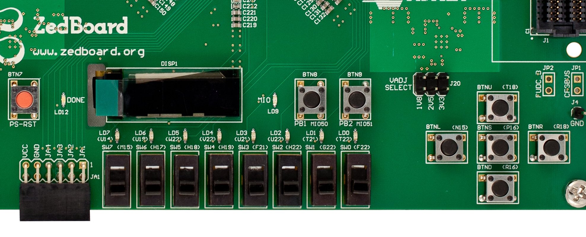
On the board, several input and output resources are available. Now we will describe how the hardware peripherals in Table 1 actually map to this board resources. Figure 1 shows a section of the board which contains most of the resources that will be used in the labs.
Zedboard LEDs
The LEDs present in the board, as seen in Figure 1, (LD0-7), shall be controlled using the AXI GPIO peripheral mapped at the memory address described in Table 1. The LEDs map directly to Channel 1 of the peripheral:
| Bit | Zedboard LED |
|---|---|
| 0 | LD0 |
| 1 | LD1 |
| 2 | LD2 |
| 3 | LD3 |
| 4 | LD4 |
| 5 | LD5 |
| 6 | LD6 |
| 7 | LD7 |
GPIO_DATA register of AXI GPIO peripheral to LED mapping
Zedboard DIP Switches
Just like the LEDs, the switches SW0-7 are directly mapped to the AXI GPIO peripheral as described in the hardware mapping table. They also use Channel 1 on the respective peripheral.
Push buttons
The push buttons are mapped to yet another AXI GPIO peripheral’s channel 1. Please consult the mapping table for the base address. The push buttons are mapped as follows:
| Push Button | Bit |
|---|---|
| BTNU | 4 |
| BTND | 1 |
| BTNR | 3 |
| BTNL | 2 |
| BTNC | 0 |
Push button register mapping
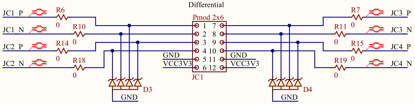
PMOD Connectors
The PMOD connectors are headers that expose several I/O ports of the FPGA to the external world. We will be using a few of those to output different types of signals. Figure 1 shows only one of those (JA1), however we will be using more headers during the course.
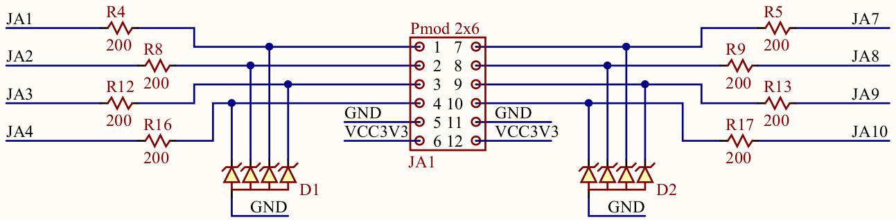
The PMOD signals are mapped as follows:
| PMOD Header | Signals | Hardware peripheral | Description |
|---|---|---|---|
| JA1 | JA{1,2,3,4,7,8,9,10} | PMOD GPIO, Channel 1 | Additional input / output signals |
| JB1 | JB{1,2,3,4,7,8,9,10} | PMOD GPIO, Channel 2 | Additional input / output signals |
| JC1 | JC1_P | Timer 0 | PWM output signal from Timer 0 |
| JC1 | JC1_N | Timer 1 | PWM output signal from Timer 1 |
| JC1 | JC2_P | Timer 2 | Capture input signal to Timer 2 |
| JC1 | JC2_N | Timer 2 | Generate output signal from Timer 2 |
| JC1 | JC3_P | UART RX | UART RX signal |
| JC1 | JC3_N | UART TX | UART TX signal |
PMOD Header signal mapping
OLED Display
The OLED display present in the board can be controlled by user applications. It requires the use of two different interfaces for full control; data is transmitted using the SPI (serial peripheral interface) OLED peripheral and also the initialization sequence requires I/O interaction which is controlled by the Channel 2 of the LED AXI GPIO peripheral.
Timers and PWM
There are three timers present in the hardware plaform:
| Name | Function | Signal destinations |
|---|---|---|
| Timer 0 | PWM output | PMOD and/or LD0 |
| Timer 1 | PWM output | PMOD and/or LD1 |
| Timer 2 | Input capture | PMOD |
Timers and signals
Please refer to the signal multiplexing section for details on how to output the PWM signals from Timers 0,1 to the LEDs.
Whereas Timers 0 and 1 can generate PWM signals, Timer 2 is configured for input capture events.
All timers are clocked using a 100 MHz clock.
Signal Multiplexing
The special AXI Signal Mux devices control the signal path that goes to two of the LEDs: LD0 and LD1. By manipulating the memory mapped registers, one can select either the PWM output signal from Timer 0 and Timer 1 respectively, or the regular signal from the LED GPIO controller.
Using the multiplexer
This peripheral does not have a datasheet; in fact its usage is so simple that it does’t need one, as there is only one register present.
The usage is extremely simple:
-
Write the value 0 to the base address to have the GPIO signal from the LED GPIO peripheral outputted to LD{0, 1}
-
Write the value 1 to the base address to have the PWM signal from Timer{0, 1} outputted to LD{0, 1}
-
Any other values written will make the LED always be OFF.
Reading and datasheets
AXI GPIO Datasheet https://www.xilinx.com/support/documentation/ip_documentation/axi_gpio/v2_0/pg144-axi-gpio.pdf
AXI Timer Datasheet https://www.xilinx.com/support/documentation/ip_documentation/axi_timer/v2_0/pg079-axi-timer.pdf
AXI Quad SPI Datasheet https://www.xilinx.com/support/documentation/ip_documentation/axi_quad_spi/v3_2/pg153-axi-quad-spi.pdf
ZedBoard Schematic https://www.xilinx.com/support/documentation/university/XUP%20Boards/XUPZedBoard/documentation/ZedBoard_RevC.1_Schematic_130129.pdf
AXI UART Lite https://www.xilinx.com/support/documentation/ip_documentation/axi_uartlite/v2_0/pg142-axi-uartlite.pdf